During the last few years, the semiconductor industry encountered a phase of crisis aggravated by a steep decline in PC sales, silicon shortage, geopolitical tensions, and the global COVID-19 pandemic, causing supply chain disruption. Such scenarios led to the shutdown of numerous chip manufacturing plants and factories across the globe. Despite confronting these challenges, the industry is following an upward trajectory, expecting to reach a valuation of USD 588 billion in 2024 from USD 526.8 billion in 2023. The industry’s significant growth potential is attributed to AI integration and the rising demand for consumer electronics and connected devices.
Is Semiconductor Engineering Pivotal for Advancing the Electronics Sector?
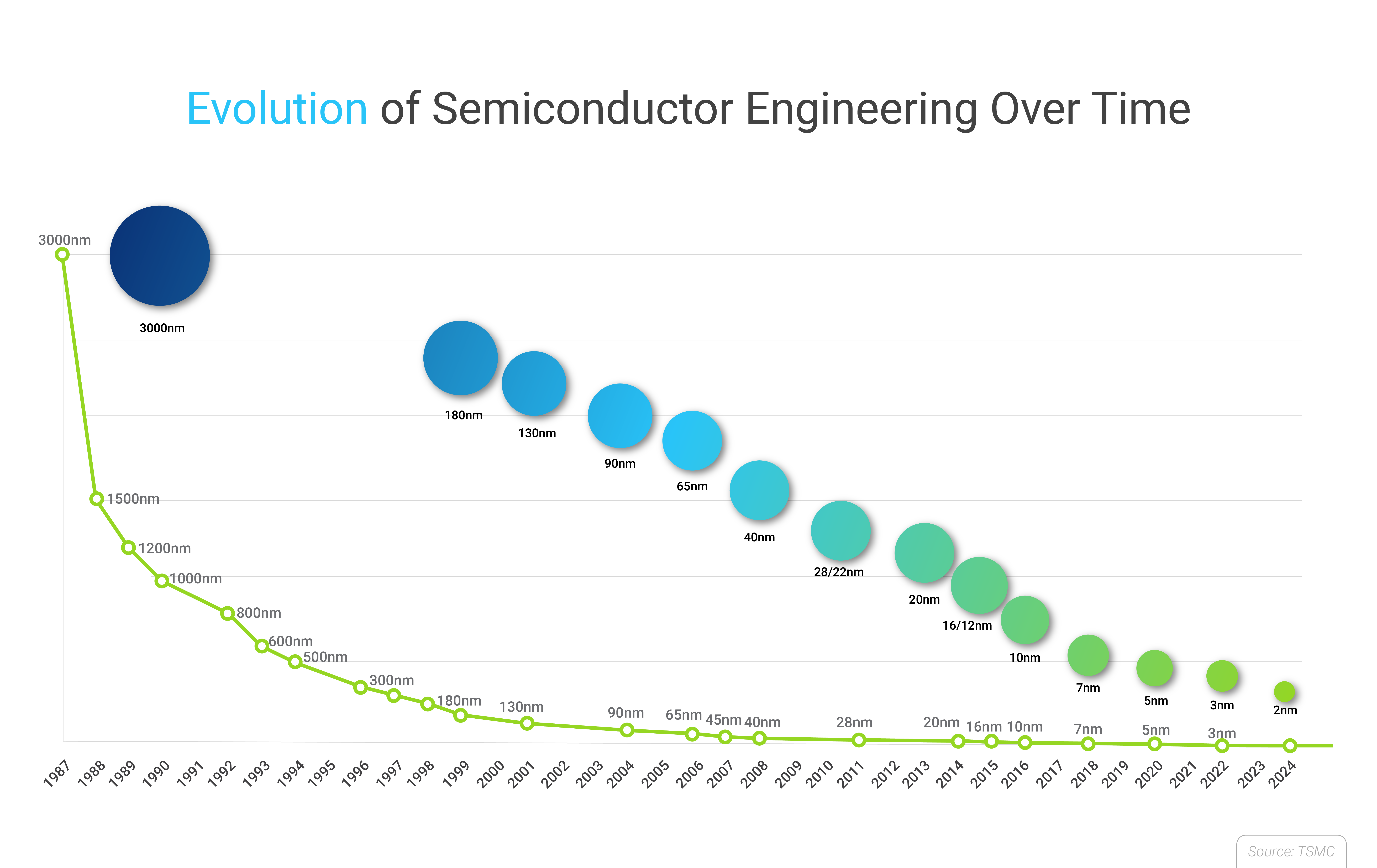
In the dynamic realm of electronics, semiconductor engineering shines as the guiding star, illuminating innovation and powering the smart world. The development of ultra-speed and power-efficient customized processors involves high-grade semiconductor engineering. The companies have been fabricating innovative approaches to miniaturize chipsets and integrating software (firmware) with hardware (chips) in order to optimize and accelerate the hardware performance by multiple folds. The real-world example includes the N3P and N3X technology roadmap unveiled by TSMC last year for fabricating advanced 3nm node technology processors.
Top Three Trends in Semiconductor Engineering
As semiconductor digital engineering is crucial in further elevating the chipset performance, the three key semiconductor next-gen engineering trends that are leading to innovations and new players entering the marketplace are:
Disaggregated Chips
In 2024, disaggregated chip designing aims to create a buzz in multiple sectors, responding to an unceasing requirement for IoT (Internet of Things). Various tech giants are aggressively working on establishing in-house chip manufacturing architectures. This trend will likely diversify the pathways of fabless players and third-party silicon IPs to introduce new products faster and cheaper. Chips with in-built quality third-party IPs verified at the chiplet level can undoubtedly offer a faster go-to-market (GTM) strategy.
Impact
- Significantly fast development process
- Over 10x reduction in bugs
- Opportunity to re-claim the IPs across multiple commodities
Packaging Innovation
Despite Moore’s law, which predicted that the transistor count on a microchip would double every two years, node advancement is reaching its limits at such a nanometer scale. Front-end chip manufacturing technical advances are slowing down, and the economically viable maximum die size (and thus performance) is becoming restricted. System-on-a-chip (SoC) packaging has emerged as a solution that integrates various components from different wafers into a single chip, optimizing performance and power efficiency.
Impact
- Enhanced computational power
- Reduced die cost and complexity
- Optimized heat dissipation
Custom Chipsets for Other Vehicles
To incorporate connected and autonomous functionalities without compromising performance, enterprises across diversified verticals strive to build robust and custom chipsets that deliver exceedingly capable outcomes. To justify, Apple introduced the M1 chip for its 2021 edition of PCs, ditching Intel microprocessors to get rid of dependency and unlock more chipset-related features.
Also, several automotive companies are in line to fabricate their own chipsets by 2025 to manufacture smarter EVs, eradicating the impact of supply chain disruption.
Impact
- Decoupling of hardware and software
- Reduced complexity
- Supply chain resilience
Conclusion
Digital engineering will continue redefining the semiconductor vertical, thereby encouraging cross-domain enterprises to automate their products & processes in the coming years. The blog emphasizes the importance of ultra-speed and power-efficient customized processors across SMEs and multinational corporations. To learn more about how Ingenious e-Brain supports enterprises in plotting the appropriate path toward digital engineering, reach out to our competent experts by either filling out the below form or emailing us at contact@iebrain.com.