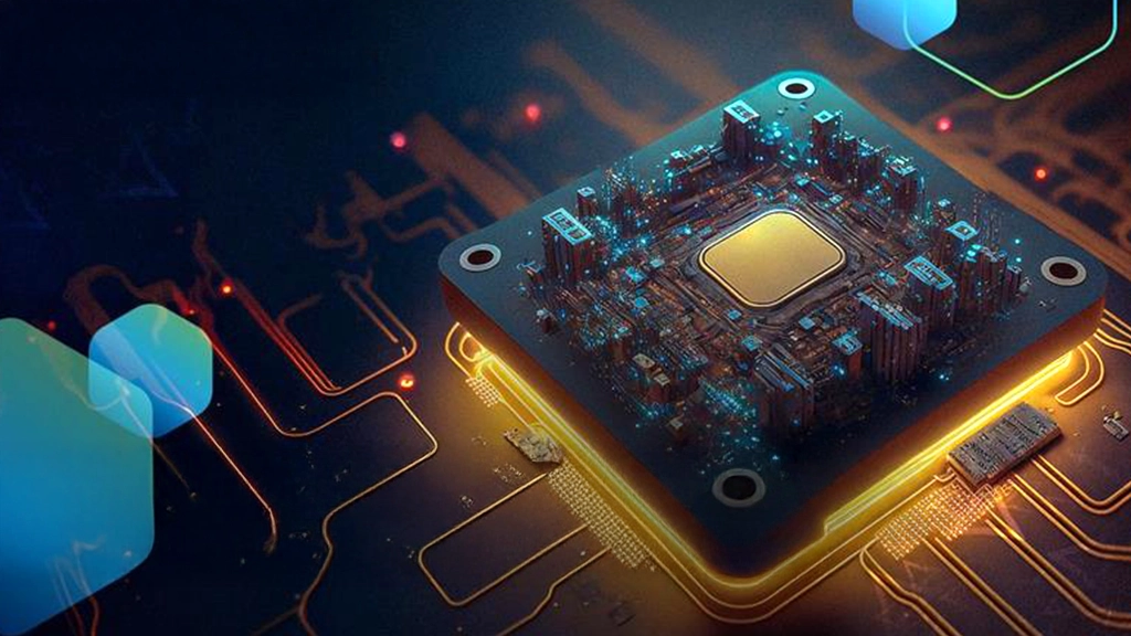
Advanced semiconductor packaging is evolving from a focus on transistor shrinkage to how effectively semiconductor devices are connected (interconnected), stacked (3D), or combined (heterogeneous). As advanced packaging evolves toward the use of “chiplets” to allow multiple functions to be placed together, toward 3-dimensional stacking, and toward heterogeneous integration; the limits of current organic substrates are being realized. In this context, glass core substrates are evolving not as an evolutionary step toward better materials but as a fundamentally new material that meets the physical performance needs of future systems.
From Material Limitation to Material Alignment
Traditional organic substrates have been adequate for the industry, but they are now showing significant limitations in high-frequency and high-density environments. Warping, dielectric loss, and thermal mismatch cannot be managed as trade-offs anymore in AI accelerators and high-performance computing applications.
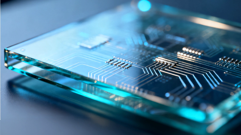
Glass represents an entirely new equation. With an extremely flat surface, minimal dielectric loss, and identical thermal expansion characteristics to silicon, glass provides the ability to make smaller geometries and reliable connections. It is the inherent nature of these characteristics to improve the yield, signal quality, and long-term reliability of semiconductor devices.
That is why leading technology companies such as Apple, NVIDIA, and AMD are increasingly linking their advanced packaging road maps with glass substrates specifically for high-end AI and HPC workload applications, where the electrical margin for error is very thin.
Hybrid Bonding and Glass: A Converging Innovation Stack
There is a parallel innovation stack happening technically; hybrid bonding. This advanced semiconductor packaging technique replaces traditional solder-based interconnects with direct copper-to-copper bonding, allowing for much greater interconnect density and shorter electrical paths.
On glass core substrates, hybrid bonding achieves maximum benefit. The dimensional stability of glass provides precision placement during bonding and minimizes signal degradation. This synergy is especially useful in supporting chiplet architectures and 3d stacking, where interconnect efficiency is directly proportional to computational performance.
Ultimately, glass core substrates and hybrid bonding are not independent innovations; they represent two sides of the same coin.
Market Dominance of Top Players Shaping Industry Dynamics
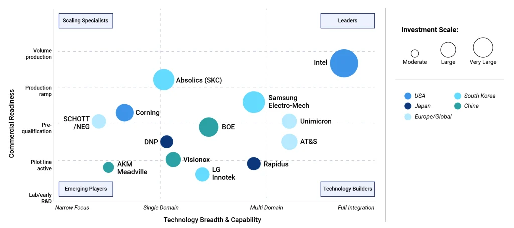
The glass core substrate market is highly concentrated, with several companies controlling almost all global supply. What differentiates these companies is their strategic positions regarding advanced semiconductor packaging.
AGC Inc. has emerged as a leader due to continuous advancements made by the company in customizing glass formulations for semiconductor applications. The company is partnering with foundries to enable glass core substrates for 2.5-dimensional and 3-dimensional packaging, particularly in high-performance computing.
Corning Incorporated is progressing with ultra-low expansion glasses designed to support higher interconnect density and improved thermal performance. Corning’s focus is on next-generation data centers and AI workloads.
Schott AG is utilizing its experience in specialty glasses to develop substrates for high-reliability applications, including automotive and aerospace electronics. Schott AG is also exploring hermetically sealed packaging options that increase durability.
Hoya Corporation and Ohara Inc. are establishing themselves in the marketplace by integrating closely with semiconductor ecosystems in the Asia Pacific, thereby improving supply chain efficiencies and cycle rates for innovation.
New entrants into the marketplace, such as Dai Nippon Printing, are creating hybrid substrate solutions combining elements of both glass and organic materials, seeking to strike a balance between performance and cost.
Similarly, CrysTop Glass is focusing on scalable manufacturing methods to reduce semiconductor packaging and overall production costs, thereby unlocking access to larger segments of the market.
Collectively, the fact that the majority of leading firms, including Intel, Amkor, and others, control roughly 90% of global supply illustrates a very dominant firm or firms in an oligopoly situation. This group of firms defines the overall direction of the industry as well as how glass substrates fit into other advanced packaging technologies, such as hybrid bonding and heterogeneous integration. Other emerging players have been trying to break up this dominance by lowering their production cost through scaling and improving upon their manufacturing process.
Market Trajectory: Growth Anchored in Structural Demand Along With Potential Applications
The global market for glass core substrates reached $195 Million in 2024 and is projected to surpass $570 Million in 2032 at a compound annual growth rate of 17%. The growth in the glass core substrate market is being driven structurally by increased complexity for semiconductor packaging, particularly in AI, data centers, and 5G infrastructure.
As semiconductor chips become more complex, the existing approach to packaging does not meet the market needs, creating pressure to move toward materials capable of supporting higher interconnect densities, improved thermal performance and signal integrity.
AI and HPC applications are driving the glass transition. High-power density applications using chiplet architectures require substrates that can perform under extreme operating conditions, which makes glass a natural choice because of its dimensional stability and low electrical loss characteristics.
This structural shift away from organic materials is unlike previous material changes that were driven by incremental innovation in semiconductor packaging.
SWOT Analysis: Bridging Performance and Manufacturability
Market opportunities exist outside of standard electronic packaging areas, including photonics integration, where glass substrates facilitate lower-loss optical/electronic integration; automotive electronics, where reliability/thermal/environmental stability is important.
Although glass offers many benefits over traditional organic substrates, transitioning to glass substrates presents some challenges, especially in semiconductor packaging. Through-glass via formation, metallization, and other manufacturing techniques present processing challenges that are still being resolved at scale. There are yield-related issues, and the production cost for glass substrates is still twice as expensive as traditional organic materials while providing relatively lower manufacturing yields.
Additionally, the overall ecosystem must also adapt. Engineers working with glass require a completely different mindset relative to mechanical properties and failure mechanisms compared to engineers who are accustomed to designing for organic substrates. Also, since glass is brittle and sensitive to handling, modifications may be required to most assembly equipment used today. All of these factors contribute to a slow adoption curve, although one that is steady.
High production costs and lower manufacturing yields create additional market obstacles for glass substrates. Currently, glass substrates cost 2-3 times more than organic alternatives and produce comparable or even less favorable yields. Furthermore, thermal shock sensitivity in assembly processes creates yet another challenge requiring tighter process controls and longer qualification cycles.
However, all of these aspects are typical for large-scale material transitions within the semiconductor industry.
Regional Market Outlook: A Concentrated Yet Evolving Landscape
The global distribution of the glass core substrates market mirrors the larger structure of the semiconductor manufacturing industry, with Asia Pacific dominating and Western countries strategically investing. Asia Pacific accounts for approximately 52% of the global market, representing a dominant position for producing and consuming glass substrate materials.
The reasons for this dominance include:
- Proximity to semiconductor foundry sites
- Government-backed initiatives
- Presence of leading glass substrate suppliers
Japan, South Korea, Taiwan, and China each continue to aggressively invest in advanced packaging capabilities to ensure continued dominance.
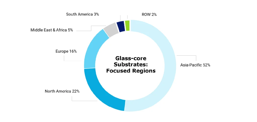
North America is home to about 22% of the market, with growth occurring mainly as a result of R&D activity and early adoption in AI and data center applications. Partnerships between innovative material suppliers and semiconductor companies are promoting faster development of glass-based packaging solutions in North America, particularly due to U.S. federal funding to develop domestic semiconductor capabilities.
At nearly 16%, Europe focuses on specialty applications, particularly in automotive electronics and industrial systems. Although volumes are low in comparison to the Asia Pacific, Europe is positioning itself for future opportunities through regulatory alignment and targeted investments in semiconductor independence.
Emerging markets in the Middle East and South America are also showing interest in glass core substrate products, accounting for almost 8% of the market share. However, growing investments in digital infrastructure and semiconductor ecosystems suggest long-term prospects, particularly as supply chain diversification becomes a global issue.
The Road Ahead: A Material Shift with System-Level Impact
Glass substrates are not merely a substitute product; they will play an enabling role in the next generation of semiconductor innovation. Compatibility with hybrid bonding; support for high-density interconnects; alignment with emerging architecture concepts position them as essential components for future systems.
As the industry continues down the path of advancing performance & integration, the utilization of glass substrate materials will continue to gain traction, driven by both technological necessity & strategic investment.
Closing Perspective
Glass core substrate materials are rapidly transforming from a niche innovation to a key enabling element for next-generation semiconductor packaging. Achieving the ultimate value of this transformation will depend upon much more than simply gaining acceptance; it will require coordination across design teams, manufacturing organizations & partners within the ecosystem.
Our team works collaboratively with industry stakeholders to help bridge the gap between technology & strategy, providing insights that convert technology complexity into actionable strategies.
To explore how our team can strategically guide you in implementing advanced semiconductor packaging strategies, connect with our experts by filling out the form below or emailing them directly at contact@iebrain.com.